Research
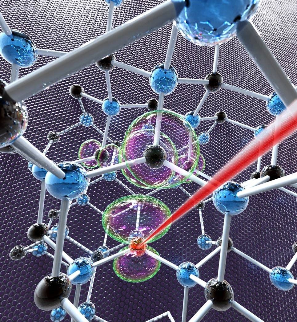
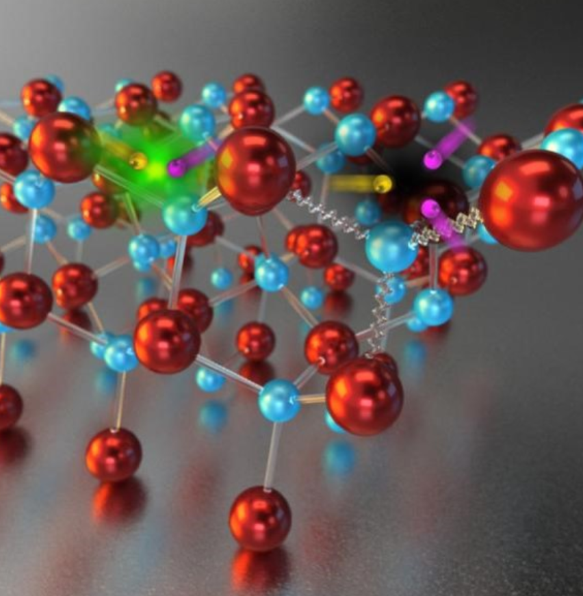
Defects for quantum information science
Identifying and designing physical systems for use as qubits, the basic units of quantum information, are critical steps in the development of a quantum computer. Among the possibilities in the solid state, a defect in diamond known as the nitrogen-vacancy (NV) center stands out for its robustness because its quantum state can be initialized, manipulated, and measured with high fidelity at room temperature. We have studied analogous defects in other materials as a way to develop a systematic approach to identify deep center defects with similar properties to the NV center. Currently, we are using this approach to analyze the properties of defects, their hosts, and their impact on quantities important for quantum computing, which includes spin-state lifetime, defect stability, and internal optical transitions.
Loss mechanisms in light emitters
Solid-state light emitters are used for general lighting, display, storage, and optical communication technologies. However, the devices suffer from loss from processes that do not generate light from injected electrons and holes. The loss mechanisms include Auger recombination and Shockley-Read-Hall recombination at defects, as well as absorption of light before it can leave the device. We are investigating these loss mechanisms from first principles in order to elucidate their microscopic origins, and provide design suggestion to mitigate their detrimental effects. We develop computational tools to address the mechanisms, and apply them to a variety of optoelectronic materials, including nitride semiconductors and hybrid perovskites.
Nitride semiconductors
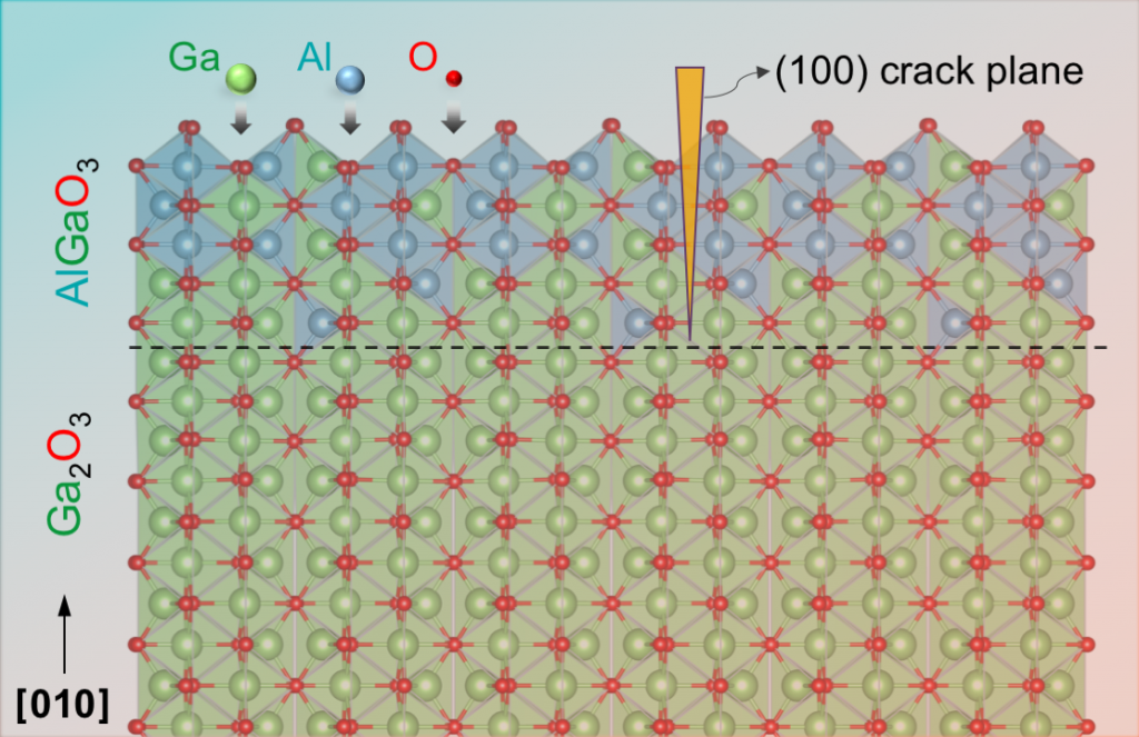
Group-III nitrides are key materials for light emitting devices as well as high power and high frequency electronics. Surface and interface structures as well as defects greatly affect the growth and doping of the materials and the performance of the devices. We are studying the interplay between structural and electronic properties of surfaces and interfaces, addressing problems related to doping and defects, studying polarization, and investigating loss mechanisms. The materials include the "traditional" wurtzite-structure III-nitrides (GaN, InN, and AlN) and their alloys, alloys with BN, and also rocksalt-structure ScN, which exhibits fascinating properties in interfaces with GaN and when alloyed with AlN.
Halide perovskites
Halide perovskites exhibit high conversion efficiencies in photovoltaics. They are easy to fabricate and can also be applied in light emitters, lasers, photocatalysts, actuators, and scintillators. Still, many questions about the underlying physical mechanisms are under debate. We perform fundamental studies of carrier recombination processes, allowing us to critically assess key concepts, and provide valuable insights. Our studies not only focus on addressing the origin of the remarkable efficiencies, but also aim at guiding improved design of optimized materials that can overcome drawbacks such as instability and toxicity.
Binary oxides
Semiconducting oxides exhibit many of the advantages of conventional semiconductors with even richer possibilities stemming from a larger diversity of structures and the availability of large single-crystal substrates for epitaxial growth. Semiconducting oxides are used for transparent electronics, sensors, high-power transistors, and many other applications. We explore bulk, surface, interface, and defect properties of various binary oxides, such as ZnO, SnO2, TiO2, MgO. Recently we have been focusing on the sesquioxides Ga2O3, In2O3, and Al2O3. Understanding the effects of dopants and native point defects on technologically relevant properties such as conductivity in these materials is crucial towards their utilization in devices.
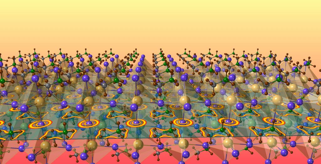
Complex oxides
Interfaces between certain complex oxides (transition-metal perovskites) have been shown to spontaneously form a two-dimensional electron gas (2DEG) with a carrier density corresponding to 1/2 electron per interface unit cell - one observes metallic behavior at the interface between two insulators. We have been working on understanding these interfaces: Where do the carriers come from, into which material do they go, how can surface terminations play a role, and why are some interfaces insulating even though they have the carrier density corresponding to a 2DEG? We have also investigated the bulk materials themselves, without the presence of an interface, as many of these perovskite transition-metal oxides are largely unexplored in the literature. Here our efforts have focused on the mechanisms determining carrier mobility, band gaps, charge localization, and the behavior of defects.
Read our popular-science account of this research topic at FunSizePhysics.com.
Hydrogen
Rising world energy demands and increased concerns about greenhouse gases provide powerful incentives for identifying alternative energy sources. Hydrogen has the potential to serve as an energy carrier at the core of a carbon-free energy system. However, producing hydrogen, as well as storing it, is a great challenges. Using first-principles calculations, we investigate the mechanisms of photochemical hydrogen generation, and hydrogen desorption, incorporation, and diffusion in novel high-capacity hydrogen storage materials.
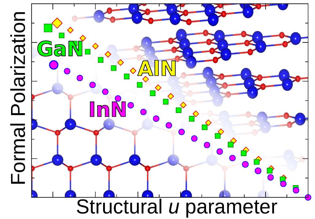
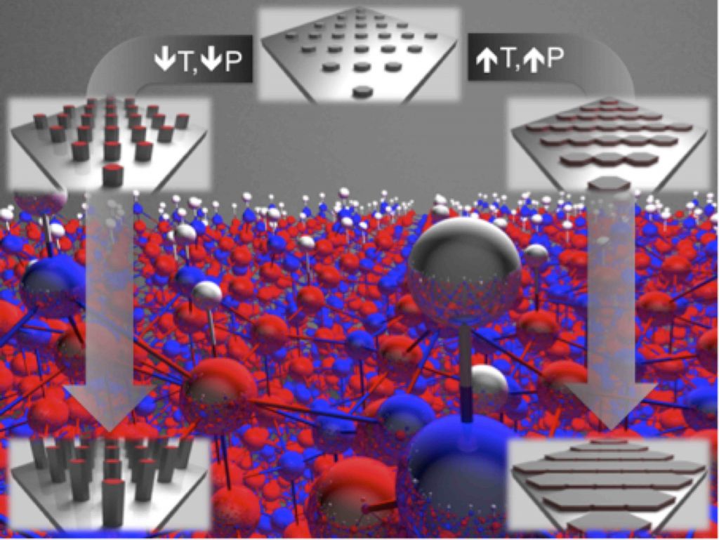
Understanding and exploiting polarization
Many materials exhibit piezoelectricity; a smaller number also display spontaneous polarization (pyroelectricity). In light emitters the presence of polarization in quantum wells is detrimental; but in electronic devices polarization can be beneficially exploited because it enhance carrier densities. We engage in fundamental studies of the physics of polarization and apply the insights to new materials combinations.