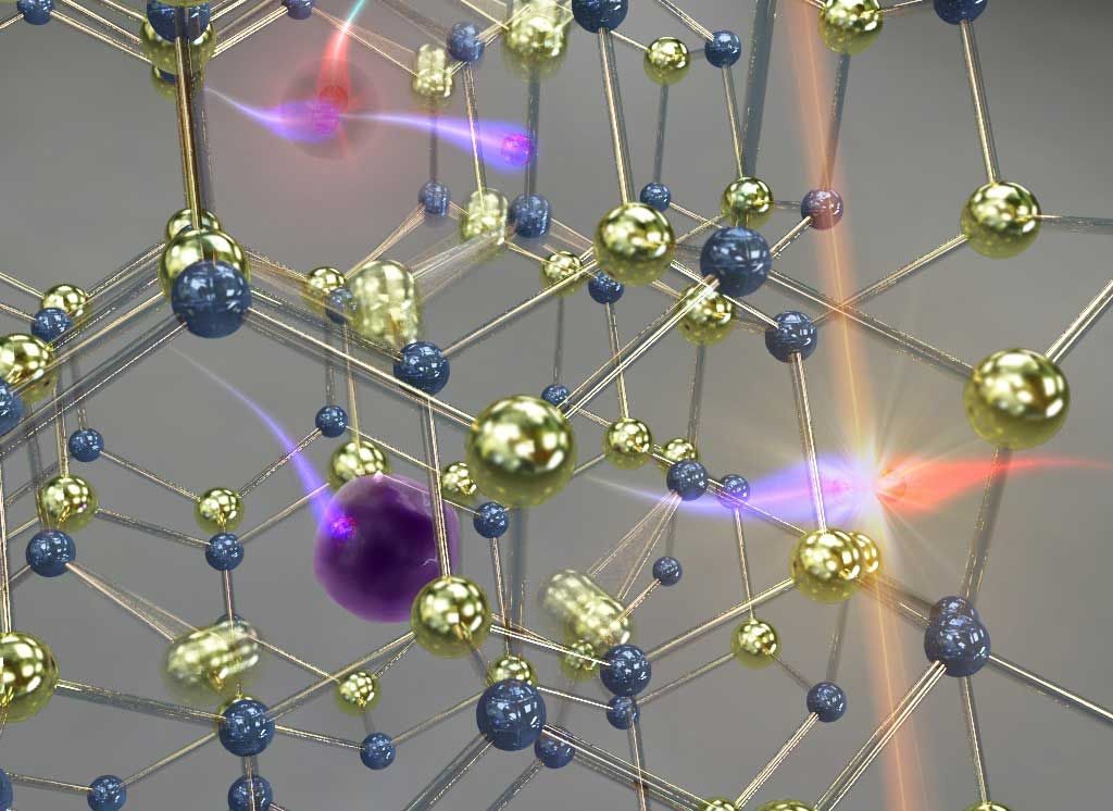
Nitride Semiconductors
Group-III nitrides are key materials for green, blue and UV light emitting devices and high-power high-frequency electronics devices. One of the most exciting applications for nitride materials is in solid-state optoelectronic devices, such as light emitting diodes (LEDs) and laser diodes (LDs). About 12 % of the United States' energy goes to lighting (http://www.eia.gov/), and LED/LD-base lighting is poised to revolutionize this market. LED bulbs are significantly more efficient than incandescents, and more environmentally friendly than fluorescents, since they do not contain harmful elements like mercury. In addition, LEDs lights allow for more intelligent lighting designs since they are dimmable and can even be adjustable over a wide range of color temperatures. The InGaN/GaN system has been demonstrated as an ideal material for high efficiency blue LEDs and LDs, and is the basis of the LED lighting industry.
Current research is pushing the output wavelength of these devices into the green and, using the AlGaN/GaN system, into the ultraviolet . Much of the ground-breaking research is occurring in the Solid State Lighting and Energy Electronics Center (SSLEEC) at UCSB. The goal of our research in nitrides is to assist this effort by providing a deeper understanding of the fundamental materials properties and mechanisms on which these devices are based, so that design, growth, and processing can be optimized. For a short summary of research being performed in our group, watch this video in which Cyrus Dreyer, a former PhD student in the Van de Walle group, explains nitrides.
Hydrogenated GaN surfaces
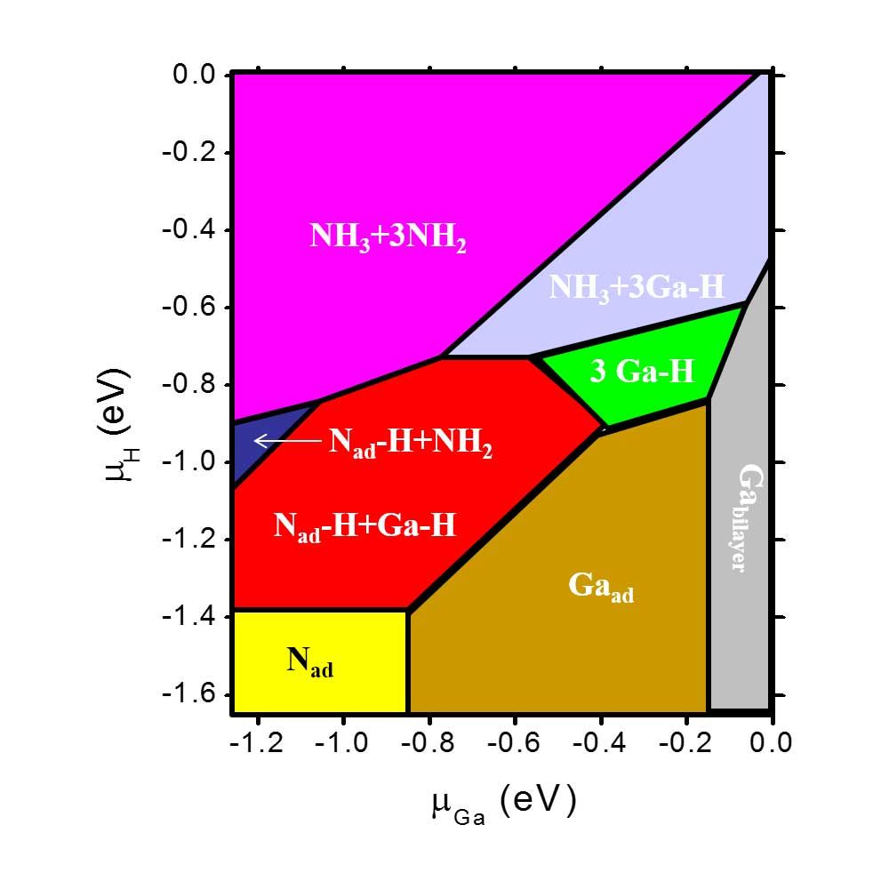
Based on density functional calculations and thermodynamic relations, the phase diagram of relevant reconstructions of hydrogenated GaN surfaces can be studied by comparing their Gibbs free energies as functions of temperature, pressure and chemical potentials. The energetic and structural properties of surfaces can be predicted under realistic conditions. [1]
Surface energies in GaN
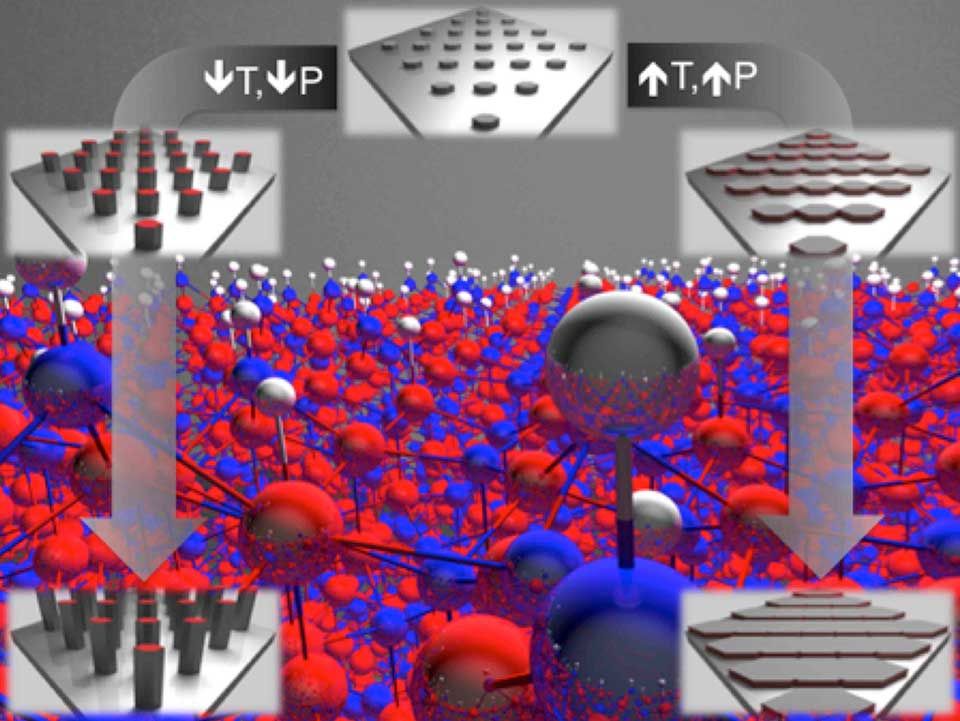
Growth of high quality single crystals and epitaxial layers of GaN is critical for producing optoelectronic and power electronic devices that reach the full potential of this material system. One of the fundamental material properties that govern growth of single crystals is the absolute surface energy of the crystallographic planes. Knowledge of these energies is required to understand and optimize growth rates of different facets in GaN, which determine bulk and selective area growth morphologies. In addition, surface energies provide brittle fracture toughnesses of the crystal, which determine the propensity for cracks to form in different crystallographic directions. We have determined such surface energies for the nonpolar m and a planes, as well as the inequivalent N-terminated (000-1) and Ga-terminated (000-1) polar c planes. These surface energies, in general, depend on the conditions to which the surface is exposed; below we have plotted the surface energies for a range of Ga chemical potential conditions for two representative growth conditions: high pressure, high temperature conditions to represent MOCVD growth, and low temperature, low pressure conditions to represent MBE growth.
Cracks are a major limitation for the growth of III-nitride bulk crystals and thick epitaxial films. The propensity for a crack to propagate on a given plane is determined by the anisotropic fracture toughness. Using first-principles surface-energy calculations, and a simple model for cracking, we have determined toughnesses for brittle fracture in GaN and AlN, for cracks on the nonpolar polar planes. Calculated critical thicknesses for AlGaN grown on GaN correctly predict the fracture planes in polar and nonpolar growth. [1]
Optical absorption loss processes in semiconductor lasers
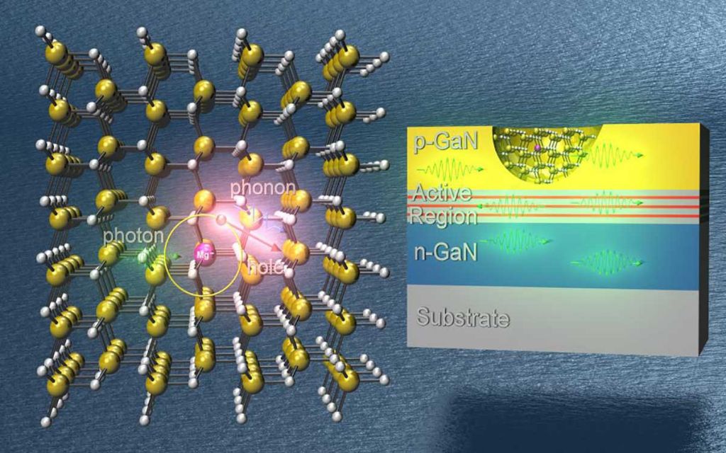
A laser video projector operates by modulating three laser beams (red, green, and blue) to project an image without the need for a screen or optical lens. Semiconductor lasers, already very successful in optical storage applications, are an ideal solution for small and portable laser projectors. Although red and blue semiconductor lasers are widely available, green ones have only recently started to emerge. However, large internal losses limit their output power. This loss is primarily due to the overlap of the optical mode with the p-type layers of the device, but its exact origin is unclear. With this question in mind, we developed a computationally-tractable first-principles formalism to study free-carrier absorption in nitride materials and assess whether it could be the microscopic mechanism responsible for the loss. [1,2] Our results show that the culprit for the optical loss is absorption by the high concentration of holes bound to non-ionized acceptor atoms (in this case Mg) in p-GaN. Although these bound holes do not contribute to the conductivity, they introduce empty states just above the valence band edge and enable optical absorption processes for every wavelength in the visible. These optical transitions are indirect, mediated by the electron-phonon-interaction which is particularly strong in the nitrides. Based on this finding, we proposed ways to reduce the absorption loss and increase the laser efficiency and power output.
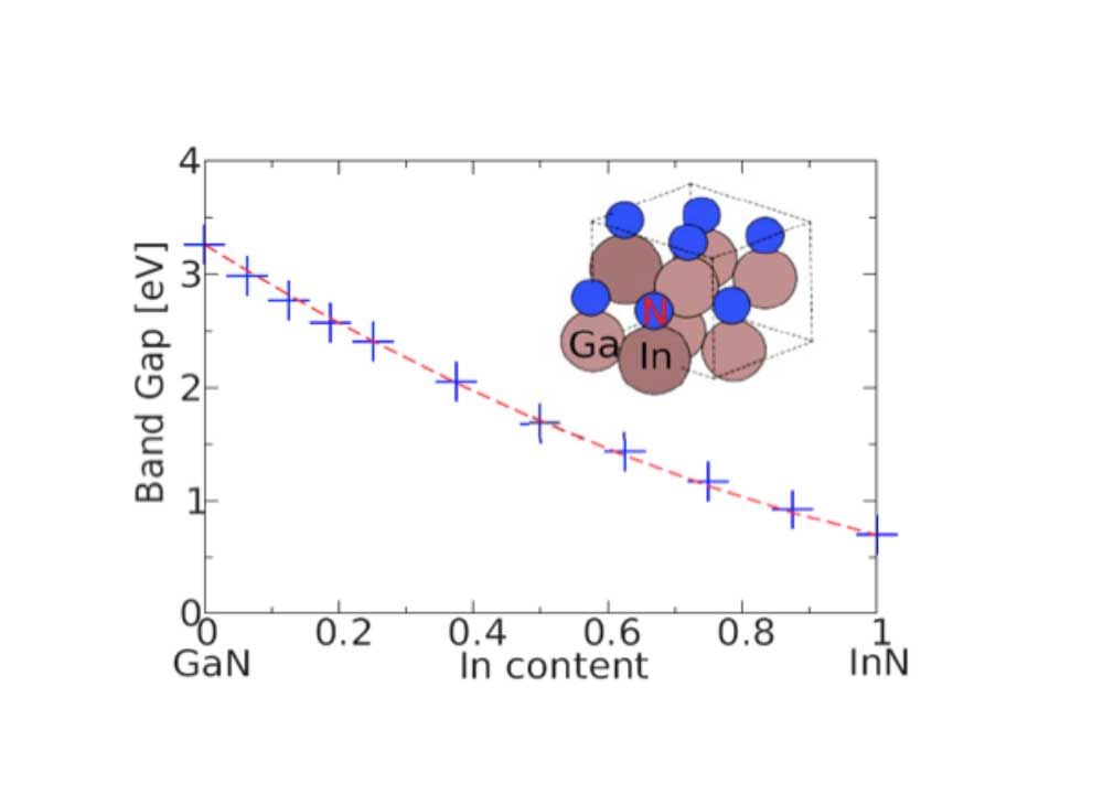
Band offsets and bowing parameters
We investigate band gaps and band alignments for AlN, GaN, InN, and InGaN alloys using density functional theory with the HSE06 exchange-correlation (XC) functional. [1,2] The band gap of InGaN alloys as a function of In content is calculated and a strong bowing at low In content is found, indicating the band gap cannot be described by a single composition-independent bowing parameter. Valence-band maxima (VBM) and conduction-band minima (CBM) are aligned by combining bulk calculations with surface calculations for nonpolar surfaces. The absolute electron affinities are found to strongly depend on the choice of XC functional, while the relative band alignments are less sensitive. We find that the VBM of InGaN alloy is a linear function of In content and that the majority of the band-gap bowing is located in the CBM. Based on the calculated electron affinities we predict that InGaN will be suited for water splitting up to 50% In content.
![Direct and indirect band gaps of BAlN alloys as functions of boron content [CB states in inset]](/sites/default/files/styles/colorbox/public/2020-09/direct-and-indirect-band-gap.jpg?itok=M34eJCTK)
Ultra-Wide-Band-Gap Nitrides
Boron nitride has been tapped as a possible candidate for extending the range of nitride alloys to even wider band gaps. The obvious candidate material for deep-UV applications is boron aluminum nitride (BAlN). We investigated the bowing of the direct and indirect band gaps of BAlN using the HSE hybrid functional. Using specifically chosen supercells to perform the explicit alloy calculations, the direct and indirect band gaps were both folded onto the zone center. We unfolded the band structure based on the wavefunction characteristics of the states in the band structure and identified the direct and indirect band gaps for each alloy supercell that was calculated. Our results indicate the bowing parameter for the direct band gap is large while the bowing parameter for the indirect band gap is significantly lower. The large bowing counteracts the direct-band-gap change from AlN to BN, making the band gap of BAlN nearly constant across the experimentally accessible range of boron concentrations. [1]
Strain effects and deformation potentials
Due to the large lattice mismatch between the substrate and the nitride overlayers, strain is always present in group-III-nitride based devices. Strain influences the energy of optical transitions and the polarization of the emitted light. The linear coefficient of the change of transition energy by strain is defined as deformation potential. The experimental determination of deformation potentials is quite difficult and the experimental data for GaN are scattered over a large range. Previous theoretical studies have also produced widely differing values and the error bars can, in part, be attributed to the band-gap problem of density functional theory. We employ the HSE06 exchange-correlation functional, which produces band gaps in good agreement with experiment. A pronounced nonlinear strain effect on band structures of nitrides is observed. [1] In the linear regime around experimental lattice parameters, we present a complete set of deformation potentials for the wurtzite phases of AlN, GaN and InN, which is essential input for device modeling. [2]