Binary Oxides
Controlling the conductivity of oxides is a formidable task, but is a fundamental step towards enabling a new range of devices . Many as-grown oxides are unintentionally conductive. For instance, ZnO and SnO2 often exhibit unintentional n-type conductivity. Because of its correlation with oxygen partial pressure, this unintentional n-type conductivity has long been attributed to oxygen vacancies. However, our first-principles calculations have shown that oxygen vacancies in these materials are high-energy defects, and do not act as shallow donors. Unintentionally incorporated impurities, such as hydrogen, are likely responsible for the observed conductivity.
Research on Ga2O3 and related materials has become extremely active. Ga2O3 has a band gap of close to 5 eV, and hence a high breakdown voltage. In spite of its large gap, it can be doped n type. High-quality substrates are available and homoepitaxial growth can be performed. All these features render Ga2O3 a prime candidate for applications in power electronics.
Gallium Oxide
Ga2O3 is one of the few wide-band-gap semiconducting oxides that remains transparent well into the ultraviolet (UV), making it promising as a deep-UV TCO. Its large band gap leads to a high breakdown field. In spite of this large band gap, Ga2O3 can be easily n-type doped. These superior properties, combined with the availability of high-quality substrates, render Ga2O3 a promising candidate for high-power electronic devices.
The Van de Walle group started working on Ga2O3 before 2010, at a time that few people recognized the potential of this material. Our early paper, many authored by Joel Varley, who was a PhD student in the group and now a Staff Scientist at Lawrence Livermore National Laboratory, laid the foundation for an understanding of band structure, point defects, and impurities.
We continue our studies of the fundamental properties of monoclinic Ga2O3 and other related polymorphs. We investigate doping, point defects, electron transport, free-carrier absorption, thermal properties, surfaces, and thermodynamics to gain a comprehensive understanding of this material. [1]
Unusual point defects
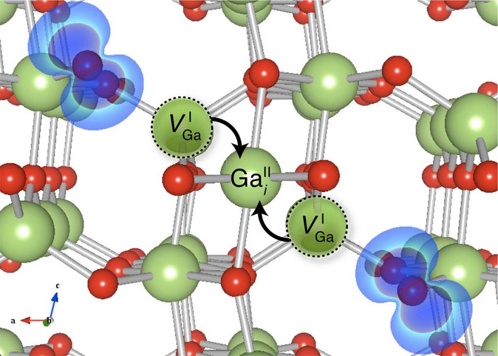
In 2011, Joel Varley predicted an unusual structure for the gallium vacancy in Ga2O3: a neighboring Ga atom moves off its substitutional site, and assumes an interstitial position. The resulting structure is a "split vacancy", which can be regarded as a complex between two vacancies and an interstitial. [1]
This might have remained an academic curiosity, until the group of Prof Jinwoo Hwang at The Ohio State University in 2019 produced beautiful transmission electron microscopy images that identified the presence of these defects in Ga2O3; one of the very few examples of direct observation of a point defect in any material. [2]
Growth of Ga2O3
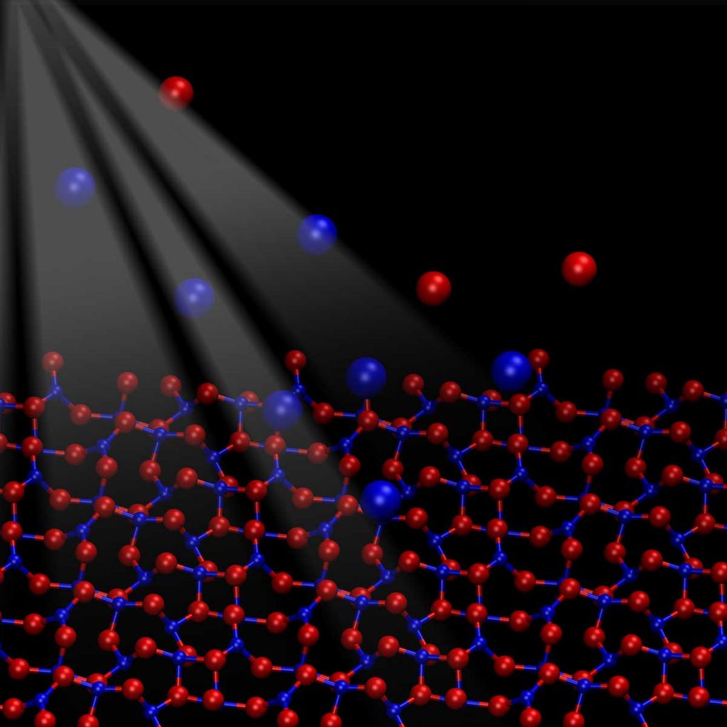
High-quality epitaxial growth of the Ga2O3 thin film is desired in order to fully exploit its potential applications. We are actively exploring the properties of the Ga2O3 (010) surface, which is the preferred growth direction in the epitaxial growth methods like plasma-assisted molecular beam epitaxy (PAMBE) and metalorganic chemical vapor deposition (MOCVD). The growth rate and crystal quality of Ga2O3 are limited by the etching of the Ga2O3 surface due to suboxide (Ga2O) formation. Experiments have shown that the growth can be improved by an additional indium supply. In order to reveal the mechanism by which In impacts growth, we use density functional theory to explore the adsorption of Ga and In adatoms on the Ga2O3(010) surface and the effect of In on the suboxide desorption. We found that the co-adsorption of In and Ga thus increases the stability of the metal-covered surface and the desorption of suboxides is suppressed in the presence of In. This happens only on the bare surface, but also in the presence of an oxygen flux, thus explaining the observed enhancement in growth rate. [1]
Critical thickness
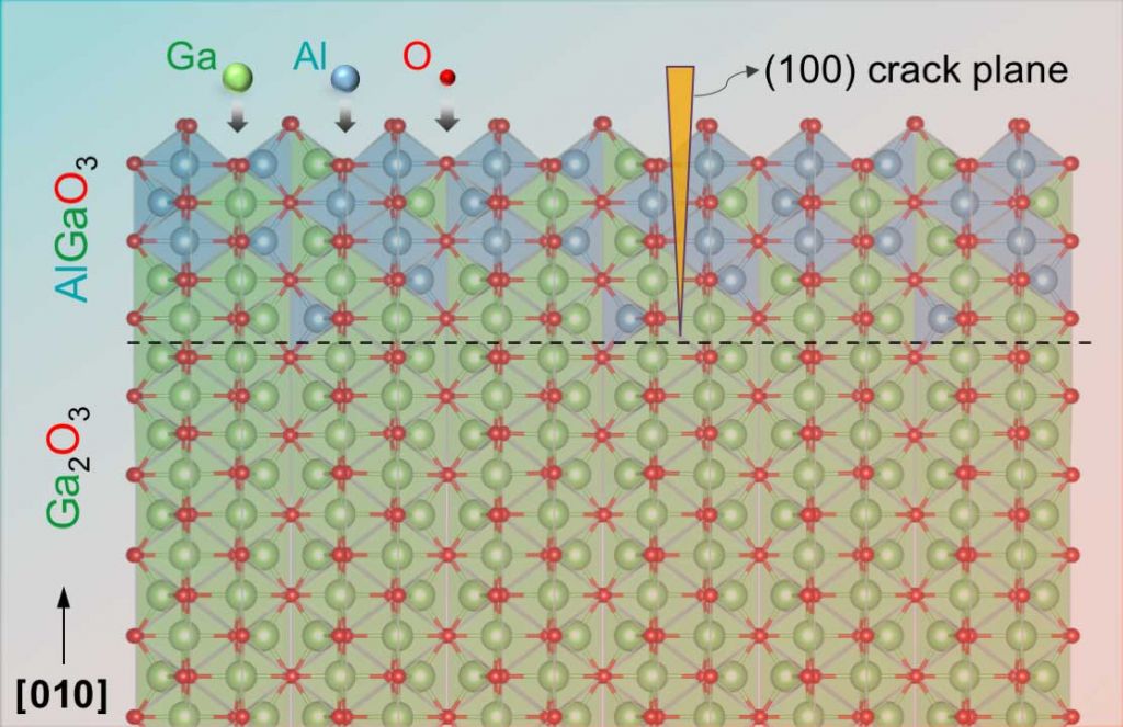
Monoclinic Ga2O3 and (AlxGa1-x)2O3 alloys are used in the fabrication of transistors for high-power electronics, enabling solid-state devices with high efficiency and large energy savings. The process involves growing the (AlxGa1-x)2O3 alloy on top of a Ga2O3 layer during the process, which can result in tensile strain and the formation of cracks in the alloy film. To understand the mechanisms by which these cracks form, we combined Griffith theory and first-principles surface calculations to determine the energy cost of forming a crack for different orientations. We were able to provide physical insights into surface stability, and to predict the maximum film thickness that can be grown before cracks appear (the so-called critical thickness). F or the most commonly used growth orientation, the [010] direction, we found that cracks will form along a (100) plane. We also predicted that film growth along a specific crystallographic direction (the [100] direction) will allow for thicker films. Our results provide important guidance for experiment. [1]
[1] “First-principles surface energies for monoclinic Ga2O3 and Al2O3 and consequences for cracking of (AlxGa1-x)2O3”, S. Mu, M. Wang, H. Peelaers, and C. G. Van de Walle, APL Materials (featured article), in press.
Zinc Oxide
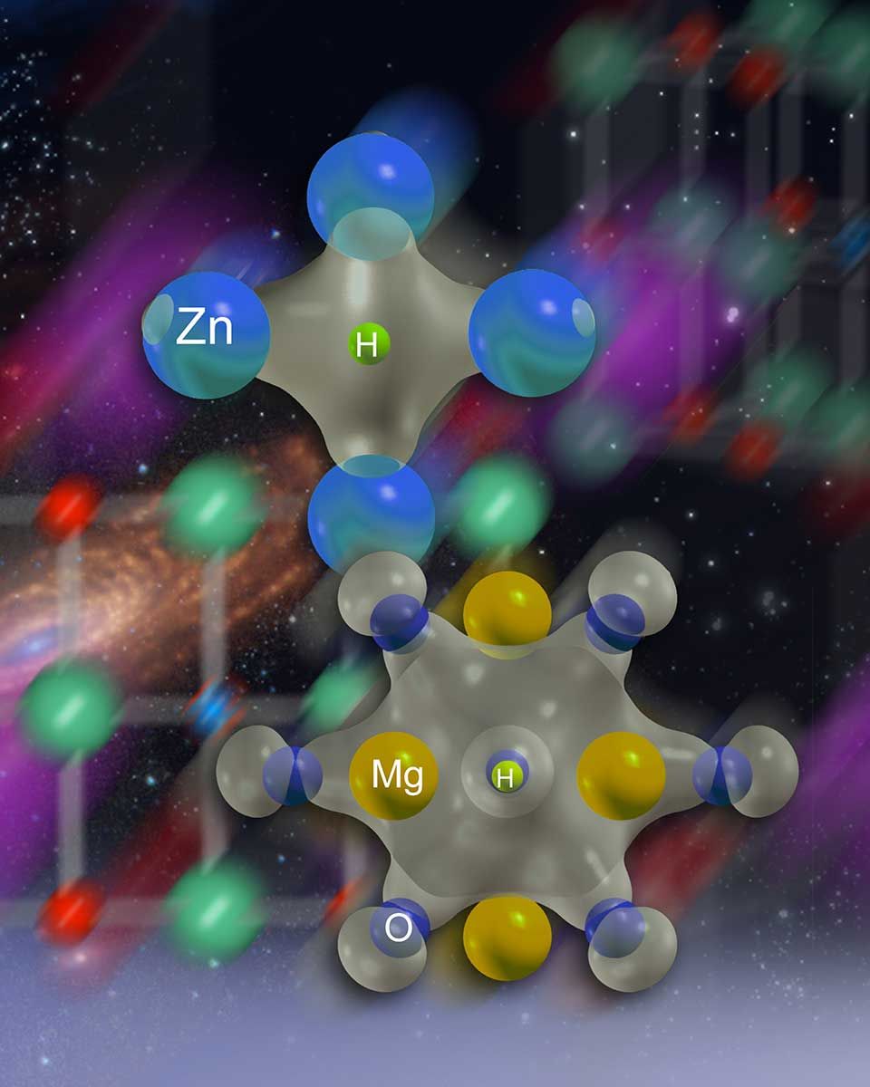
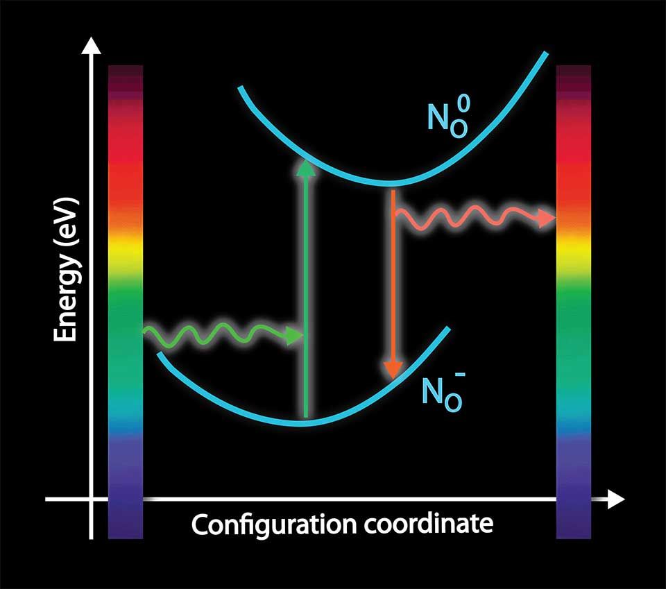
ZnO has numerous applications. Contrary to the conventional wisdom, we have shown that oxygen vacancies are deep donors with high formation energies in n-type conditions and thus not responsible for n-type conductivity. [1,2] Additionally, we have found that both interstitial and substitutional hydrogen acts as a shallow donor. Hydrogen favorably substitutes on the oxygen site, forming a multicenter bond with the neighboring Zn atoms and contributing to the observed conductivity. [3] We have performed detailed studies of all point defects and their optical activity.
p-type doping has long been attempted but has proven to be impossible in ZnO. While there are many reports claiming p-type material, all-ZnO optoelectronic devices have not been demonstrated. Nitrogen was often considered the most suitable p-type dopant, because it has been used to p-type dope similar systems (ZnSe), and it is very similar in size to O. Our calculations show that, contrary to the accepted view, nitrogen is in fact a very deep acceptor in ZnO and cannot lead to p-type conductivity. [4]
[2] “Oxygen Vacancies in ZnO”, A. Janotti and C. G. Van de Walle, Appl. Phys. Lett. 87, 122102 (2005).
[3] "Hydrogen Multicentre Bonds", A. Janotti and C. G. Van de Walle, Nature Materials 6, 44 (2007).