Polarization
Many materials exhibit piezoelectricity; a smaller number also display spontaneous polarization (pyroelectricity). In light emitters the presence of polarization in quantum wells is detrimental; but in electronic devices polarization can be beneficially exploited because it enhance carrier densities. We engage in fundamental studies of the physics of polarization and apply the insights to new materials combinations.
Polarization in nitrides
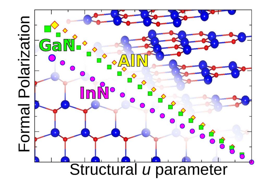
Materials with built-in electric fields, or those that can produce voltages when deformed (i.e., piezoelectric materials), have many applications, for instance as sensors, transducers, and transistors. Group-III nitrides (GaN, AlN, InN), which are also key materials in high-efficiency solid-state lighting, are important examples of such materials. When used in devices, an electric polarization (i.e., electric dipole density) is present in these materials. This fact is exploited in transistor applications, but is detrimental in lighting. The polarization properties of these and similar materials were calculated from first principles nearly two decades ago. Cyrus Dreyer found, however, that those calculated values have been misinterpreted when used to model the properties of devices. We now provide a rigorous methodology for obtaining consistent parameters for such models.
III-nitride devices are based on thin layers of different wurtzite-structure materials grown on top of each other. Differences in polarization at the interfaces result in electric fields in the layers, affecting device performance. One contribution results from the intrinsic “spontaneous” polarization of the materials, and another from a piezoelectric term associated with the strain present in the layers. The spontaneous polarization of a given material must be defined with respect to a reference structure, and we demonstrate that it is crucial to choose this structure such that it allows consistent comparisons between materials. In addition, we point out that the piezoelectric constants must take into account the change in interface area with strain, and thus should be chosen to be the so-called “improper” constants.
Our revised methodology will allow more accurate interpretation of polarization effects and more reliable modeling of heterostructure devices based on III-nitrides and other wurtzite materials. [1]
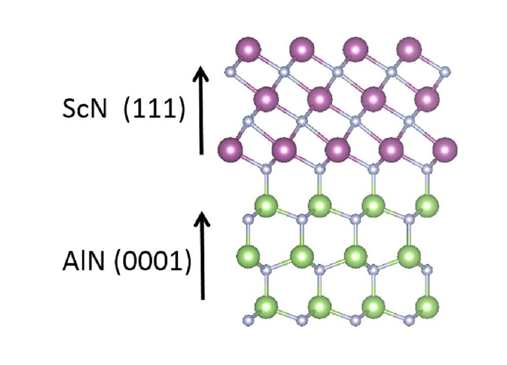
Giant polarization charge density at ScN/GaN interfaces
GaN is a wurtzite semiconductor that exhibits a large spontaneous polarization, while ScN takes the nonpolar rocksalt crystal structure. Due to the small lattice mismatch between ScN and GaN, it is possible to create a polar-nonpolar interface between the two materials.
Using density functional theory and the Berry-phase method, we examined the formal polarization of rocksalt ScN along the [111] direction, finding a polarization discontinuity of -1.388 Cm-2. We confirmed this finding with explicit ScN/GaN supercell calculations. The polarization discontinuity causes a high-density electron gas to form on the N-polar GaN/ScN interface, and a hole gas on the Ga-polar interface, with carrier concentrations up to 8.7 x 1014 cm-2. The large polarization difference and low lattice mismatch make ScN a promising material for integration with III-nitride electronic and optoelectronic devices. [1]