High-k Dielectrics
The use of high-k gate oxides such as ZrO2 and HfO2 for continued downscaling of Si-based MOS (metal-oxide-semiconductor) devices has attracted considerable attention, since MOS technology based on the traditional gate dielectric, SiO2, is meeting its scaling limit. However, the lower quality of Si/high-K interfaces remains an obstacle, and the MOS structures suffer from the presence of fixed charge and carrier traps. We are studying the properties of defects in these materials to determine which specific defects could be responsible this behavior. By calculating band alignment of the gate oxide with the channel material, we predict the position of the defect and dangling bond levels with respect to band edges of Si or III-V semiconductors, allowing an assessment of the impact of these defects on device performance.
J. L. Lyons, A. Janotti and C.G. Van de Walle, Microelectronic Engineering, 88(7), 1452-1456 (2011)
Germanium
Due to its large hole mobility, Ge is a good candidate for a high mobility channel material in novel CMOS devices. However, experimental evidence indicates that Ge MOSFETS have defects that trap charge at the channel/gate interface. Our work has focused on studying dangling-bond defects in Ge, the same defects that are the predominant defects at the Si/SiO2 interface. We have found that the electronic state associated with the Ge dangling bond lies within the valence band, making Ge dangling bonds negatively charged. This explains the absence of observations of Ge dangling bonds at Ge/oxide interfaces with electron spin resonance, which is only sensitive to neutral dangling bonds. The resulting negative fixed charge at the interface may also be responsible.for the poor performance of n-channel MOSFETs. In addition, our calculations show that interstitial hydrogen is exclusively an acceptor and therefore negatively charged in Ge. This explains why attempts at hydrogen passivation of defects at Ge/oxide interfaces have proven unsuccessful.
J. L. Lyons, A. Janotti and C.G. Van de Walle, Microelectronic Engineering, 88(7), 1452-1456 (2011)
III-V Compounds
The down scalling of CMOS device dimensions has triggered the search for novel channel materials and gate dielectrics with higher electrical permittivity needed to maintain small gate leakage. In this context, we are investigating the electronic structure of surfaces, interfaces and defects in novel semiconducting materials as well as high-k gate-dielectrics. Our studies for dangling bond defects in Ge have revealed that these defects are always negatively charged, thus explaining a number of experimental puzzles. For other channel materials such as GaAs, InAs and their alloys, we are studying their interfaces with gate dielectrics such as Ga2O3, Al2O3, and In2O3. We are also investigating defect formation and its role in Fermi-level pinning at the semiconductor-channel/gate-dielectric interface.
J.R. Weber, A. Janotti, C.G. Van de Walle, Microelect. Eng. 86, 1756 (2009)
Oxide-Nitride Interfaces
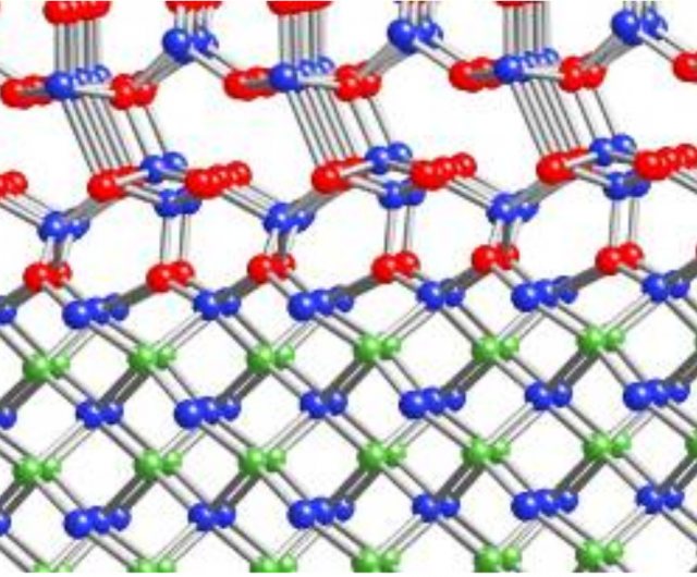
AlGaN/GaN interfaces have been exhaustively studied for the last decade due to numerous promising applications; specifically, high-electron-mobility transistors (HEMTs). Any effective realization of this will depend on the level of control over the two-dimensional electron gas (2DEG) at the interface. Surface states have been identified as the primary source of the 2DEG, and first-principles simulations have been performed on numerous different (invariably oxidized) GaN and AlN surfaces. The stability of such structures is determined via oxide-stoichiometry matching and the electron-counting rule. This is used to explain the observed dependence of electron density on thickness and barrier height in AlGaN/GaN HEMTs.
M. Miao, A. Janotti and C. G. Van de Walle, J. Appl. Phys. 107, 123713 (2010)
